
Orbit Noise Generator Wireless Board (WiBo)
Table of Contents
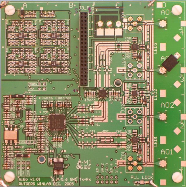
WiBo is a RF front-end board for Orbit Noise Generator designed around a Maxim, Inc. MAX2829ETN+D radio transceiver chip. Schematic is attached. It is capable of operating in one of three ISM frequency bands, namely 4900-5300 MHz, 5400-5875 MHz or 2400-2500 MHz that correspond to the IEEE 802.11 a/b/g world-wide standards, respectively. BiBo’s ADC (analog-to-digital conversion) and DAC (digital-to-analog) conversion comes from an Analog Devices AD9860 MxFE processor. Digital RADIO_IO_x signals come from a Xilinx Spartan 3. It is manufactured as a 4.00 x 4.00” printed circuit board (PCB).
Hardware Components
MAX2829ETN+D Transciever (U1)
The MAX2829 is a complex multifunction radio transceiver chip that incorporates most of the radio functions except for the reference oscillator, baseband I/Q amps, power amps and antenna switches. Please refer to the [attachement:MAX2828-9ds.pdf data sheet] and eval board notes for more information (also check http://www.maxim-ic.com/quick_view2.cfm/qv_pk/4532). Chip configuration is done by BiBo over the serial bus:
| BiBo function | WiBo function | MAX2829 function |
| RADIO_IO_1 | *CS | Chip Select, active low |
| RADIO_IO_3 | SCLK | Serial ClocK |
| RADIO_IO_4 | DIN | Data IN |
On power up and without programming the MAX2829 is in a low power “all off” state. The internal LO will lock to 2437 MHz but all input and output signals will be disabled. Current draw will be around 200-240 mA.
RF Control Register (U2)
74HC595 is an 8bit serial in parallel out shift register used to provide control signals for various RF functions. Register programming signals (U2 shares serial clock - RADIO_IO 3 and data line - RADIO_IO 4 with MAX2829):
| BiBo function | WiBo102 function | 74HC595 function |
| RADIO_IO 2 | U2 RCK | Register U2 output |
| RADIO_IO 3 | U2 SCK | Serial Clock |
| RADIO_IO 4 | U2 SER | Serial Data In |
This register controls five functions, namely, turn on/off of the 2GHz and 5GHz power amps, MAX2829 transmit and receive control signals and the MAX2829 shutdown. The register bit assignment is given in the following table:
NOTE: 0 is the first bit in, so shift in reverse order
| 01234567 | Function |
| 1xxxxxxx | turn MAX2829 on (/SHDN) |
| x1xxxxxx | turn MAX2829 TX on (TXENA) |
| xx1xxxxx | turn MAX2829 RX on (RXENA) |
| xxx1xxxx | 5G PA: 5GHZ power amp on |
| xxxx1xxx | 2G PA: 2GHz power amp on |
| xxxxx1xx | SPARE 1 output on |
| xxxxxx1x | SPARE 2 output on |
| xxxxxxx1 | SPARE 3 output on |
| xxxxxxxx1 | SPARE 4 output on (9th bit) |
LT1994 Baseband Amplifiers (U3xx, U4xx)
U300, U320 are high speed differential opamps (LT1994) wired in a 2nd order Butterworth filter with cutoff of 10MHz. They act as reconstruction filters for the output of the AD9862 DACs, which are current mode differential outputs of 0-20mA. These amps also DC offset their output to 1.1 VDC to optimally match the MAX2829 inputs. These amps are enabled only when TXENA is high, thereby saving about 18mA of power.
U400, U420 are buffer amps (gain=1) for the MAX2829 baseband I/Q signal outputs (which have 60k ohm output impedance). These amps provide simple 1st order RC filtering with cutoff F = 6 MHz. U400,U420 DC offset to 2.0VDC before sending the baseband I/Q signals to BiBo’s AD9860. These amps are enabled only when RXENA is high.
uPG2035 Switches (U3, U4, U5)
U3,U4 and U5 make up a switching matrix which offers several antenna diversity options. These are fast switching low-loss DPDT switches.
U5 is the TX output switch which switches 2.4 and 5.6 GHz MAX2829 outputs between two antennas A03 and A04. When LED3 is lit (power up default), the switch is “crossed” so the MAX2829 2.4 GHz output is routed to antenna A03 and 5.6 GHz is routed to A04.
U4 is the RX input switch which switches antennas A01 and A02 to both the 2.4 and 5.6 GHz MAX2829 inputs. When LED1 is lit (power up default), the switch is “crossed” so MAX2829 2.4 GHz input is routed to antenna A02 and 5.6 GHz is routed to A01.
The default design does not incorporate U3. Some soldering and jumpering is required to bring U3 into the mix which enables single antenna operation or maximum spatial antenna seperation (using A01 and A04).
AWL6951 Power amp (U6)
The AWL6951 is a dual mode (2.4 and 5.6GHz RF power amp) with enable signals and log detectors for measuring power output. U2 control signals 2G PA and 5G PA should only be enabled one-at-a-time to prevent overheating the chip. AUX_ADC_B1 and AUX_ADC_B2 measure the log detector outputs of the 2G and 5G amps respectively. The following measurements were taken,
- Pout (2.4GHz) @ 210 mA = 20.5 dBm (right on spec) Vout(logDET) = 0.727 V
- Pout(5.3GHz) @ 220 mA = 19.0 dBm (right on spec) Vout(logDET) = ?
- Pout(5.9GHz) @ 220 mA = 15.0 dBm (-3 dB off spec) Vout(logDET) = ?
Current draw is that of just the power amp and RF power measured at output of SMA connector when 100kHz modulation is transmitted. Otherwise MAX2829 and other circuitry draws about 170mA so total is about 480-500 mA. NOTE! It is VERY easy to over drive the power amp at either 2.4 or 5.6 GHz. This causes an UNUSUALLY high current draw by the power amp, WATCH IT !
Reference Oscillator (U9)
U9 is a 40 MHz VCXO reference oscillator. Measured frequency standard deviation over a 10 second period is about 10 Hz. AUX_DAC_B controls the frequency offset pin. This can adjust any gross frequency offsets that may exist between different WiBos. Resistors R221 and R222 act as a 10:1 divider of AUX_DAC_B so the total frequency deviation may be adjusted up or down by changing R221/2.
The default measured frequency range is approx. 550Hz/volt at 40 MHz. At 2.4GHz the frequency control will be approx. +-42kHz or 330 Hz/step of AUX_DAC_B. At 5.6GHz the frequency control will be approx. +-100kHz or 780 Hz/step.
WIC2450A Antennas (A01-A04)
Four antennas (A01-A04) are mounted directly to WiBo102 though provision is made for adding SMA connectors and using off-board antennas if necessary. Two antennas are primarily for transmission (Tx) and two for receiving (Rx). Antenna switching is possible for diversity gain. It is also possible to switch all Tx and Rx signals into a single antenna. All four antennas are WIC2450A low-cost dual mode 2.4 – 2.5 GHz and 4.9 – 6.0 GHz SMD dipoles with peak gains of 2dBi and 3 dBi respectively.
PCB
The PCB is a 4.00 x 4.00” FR-4 four-layer controlled impedance stackup board manufactured by Advanced Circuits, Inc.(http://www.4pcb.com/index.htm). For orientation purposes, reference marks are shown along the top (A-D) and right sides (1-4) of the board in one inch increments.

Looking from the top down, the top copper layer is the component side with all the high-frequency RF transmission lines. The dielectric under this layer is 20 mils thick. The structure of the traces is coplanar waveguide with ground (CPWG). A trace width of 30 mils and gap-to-ground of 18 mils provides a very close match to a 50ohm characteristic impedance.
The next copper layer down is all ground plane. The third layer down is a signal layer with predominately vertical traces surrounded by ground plane. The fourth or bottom layer is another signal layer with predominately horizontal traces.
Programming Notes
Assuming the MAX2829 has already been programmed, to enable a TX RF output the user must program a 11001xxx into U2.
NOTE: Do not turn on both the 2GHz and the 5GHz power amps at the same time!
NOTE: Do not turn on both the RXENA and TXENA lines.
Appendix
Connector J3
This is a 40-pin 2mm dual-inline connector which mates BiBo’s control signals, +3.3 VDC power and ground to WiBo.
| WiBo function | J3_F function | pin# | pin# | J3_F function | WiBo function |
| hi-speed MAX2829 TXBBQ- | DACB- | 2 | 1 | 3.3VA | |
| hi-speed MAX2829 TXBBQ+ | DACB+ | 4 | 3 | GND | |
| hi-speed MAX2829 TXBBI- | DACA+ | 6 | 5 | 3.3VA | |
| hi-speed MAX2829 TXBBI+ | DACA- | 8 | 7 | GND | |
| phase modulation of U23 | AUX_DAC_C | 10 | 9 | 3.3VA | |
| ref osc VCXO frequency adjust | AUX_DAC_B | 12 | 11 | GND | |
| PLL speed up monitor | AUX_DAC_A | 14 | 13 | 3.3VA | |
| ½ supply voltage | AUX_ADC_A1 | 1 | 15 | GND | |
| RSSI from MAX2829 | AUX_ADC_A2 | 18 | 17 | N/C | |
| 2GHz power amp detector | AUX_ADC_B1 | 20 | 19 | 3.3VD | |
| 5GHz power amp detector | AUX_ADC_B2 | 22 | 21 | GND | |
| hi-speed MAX2829 RXI+ | ADCA+ | 24 | 23 | 3.3VD | |
| hi-speed MAX2829 RXI- | ADCA_ | 26 | 25 | GND | |
| hi-speed MAX2829 RXQ+ | ADCB+ | 28 | 27 | 3.3VD | |
| hi-speed MAX2829 RXQ- | ADCB- | 30 | 29 | GND | |
| MAX2829 /CS | RADIO_IO 1 | 32 | 31 | 3.3VD | |
| U2 RCK | RADIO_IO 2 | 34 | 33 | GND | |
| MAX2829 SCLK and U2 SCK | RADIO_IO 3 | 36 | 35 | RADIO_IO 8 | MAX2829 LD (lock=1=LED on) |
| MAX2829 DIN and U2 SER | RADIO_IO 4 | 38 | 37 | RADIO_IO 7 | U5 switch(straight=0,cross=1) |
| U3 switch(straight=0,cross=1) | RADIO_IO 5 | 40 | 39 | RADIO_IO 6 | U4 switch(straight=0,cross=1) |
Optional Features
Circuit U23 makes up a reference clock phase shifter which is adjusted by AUX_DAC_C. AUX_DAC_C controls the voltage on a varactor which in turn adjusts the phase of the reference clock. Some jumpering and trace cutting is required to effect this optional circuit.
AUX_DAC_A can control the PLL CP output of the MAX2829 to effect faster lock times. This might be done with a look up chart or an available ADC could be used to implement a Wiener or Kalman filter.
Filters F70, 71, 72 and 73 are receive filters (Murata LFB or LFD or TDK DEA type) intended to channel select either 2.4 or 5.6 GHz. Similarly F60 and F61 can be used used to limit spurious output of the TX. By observation, the TX spurs are very far down and do not need filtering. By design default, none of these filters are populated on WiBo (they are hard to get in quantities less than 10,000!).
Attachments (7)
- WiBo-103-Schematics.pdf (1.7 MB ) - added by 19 years ago.
-
MAX2828-9ds.pdf
(1.0 MB
) - added by 19 years ago.
Maxim Datasheet - UNDER NDA — NOT FOR DISTRIBUTION OUTSIDE WINLAB —
- MM74HC595.pdf (118.7 KB ) - added by 19 years ago.
- lt1994.pdf (288.1 KB ) - added by 19 years ago.
- uPG2035.pdf (148.2 KB ) - added by 19 years ago.
- AWL6951.pdf (671.0 KB ) - added by 19 years ago.
- WiBo-Photo.jpg (148.2 KB ) - added by 19 years ago.